
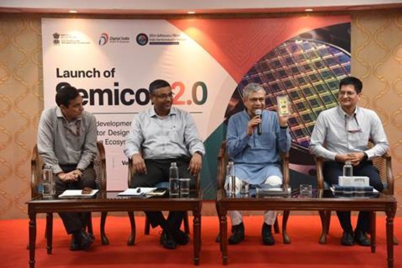
Vaishnaw said India had achieved its target of developing 85,000 semiconductor engineers over 10 years in just four years and has now set a new target of training another one lakh engineers.
“India achieved its target of developing 85,000 semiconductor engineers over a period of 10 years in just four years, and has now set a new target of developing one lakh more engineers,” Vaishnaw said.
He added that India could account for nearly 10% of the global semiconductor industry’s market in the coming years.
“In the coming years, close to 10% of the global semiconductor industry’s market is expected to be in India,” the minister said.
Highlighting the contribution of students from smaller cities, Vaishnaw said students from Tier-II and Tier-III cities had already designed more than 250 chips.
“In one case, commercial production commenced within just 13 months of the groundbreaking, while approvals were granted within 200 days, 150 days and even 90 days in multiple cases,” he said.
Vaishnaw reiterated that the semiconductor ecosystem being developed in India is expected to generate 50,000–60,000 direct jobs.
Under Semicon 2.0, supported projects will generally have a duration of up to six years, while the scheme will initially remain open for applications for three years.
The India Semiconductor Mission (ISM) will serve as the nodal agency for Semicon 2.0. It will invite applications, conduct technical and financial appraisals, recommend applicants and oversee the implementation of approved projects.
ISM may implement the design and deployment categories with assistance from the Centre for Development of Advanced Computing (C-DAC). The mission may also announce semiconductor deep-tech awards from 2026 to encourage niche innovation in the sector.